Prof. Ying Jiang’s group from Peking University built up a scanning quantum sensing microscope
Recently, Prof. Ying Jiang from the International Center for Quantum Materials and Interdisciplinary Institute of Light-Element Quantum Materials of Peking University, in collaboration with Prof. Sen Yang from the Hong Kong University of Science and Technology and Prof. Jörg Wrachtrup from Stuttgart University, successfully developed scanning quantum sensing microscope through the combination of qPlus-based scanning probe microscope (SPM) and nitrogen-vacancy (NV)-based quantum sensing. This system can obtain atomic resolution for topographic characterization and nanoscale resolution for scanning electrometry and scanning magnetometry. Meanwhile, it can also enhance the sensitivity of NV up to a single proton. This work titled “A scanning probe microscope compatible with quantum sensing at ambient conditions”, was published in the Review of Scientific Instruments on May 1st.
SPM is one of the greatest inventions in the field of nanoscience. It can obtain both topographic and physical/chemical properties of the surface at atomic scales. Unfortunately, conventional SPM struggles to detect weak electric and magnetic fields since it relies on incoherent signals such as tunneling current or atomic force. Recently NV has been proven to be a powerful quantum sensor with sensitivity even up to a single nuclear spin. Thus, one of the most promising ways to break the bottlenecks of conventional SPM is integrating the NV and advanced quantum sensing technique into SPM and developing the so-called NV-SPM. However, the present NV-SPM makes use of a cantilever or symmetric tuning fork with a large working amplitude, which leads to a tip-sample distance much larger than 1 nm and limited spatial resolution and sensitivity.
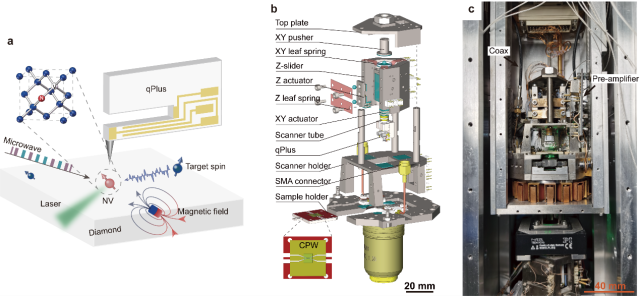
Figure 1 (a): The schematic showing the principle of scanning quantum sensing microscope, which combines the qPlus sensor and NV center and integrates laser, magnetic field, and microwave pulses for addressing and controlling the quantum states of NV. (b): The 3D model of the core component of the scanning quantum sensing microscope. (c): The photo of the core component of the scanning quantum sensing microscope.
Ying Jiang and his group, have been for a long time devoted to the development of advanced SPM systems. They have succeeded in developing a noninvasive SPM imaging and spectroscopic method by probing weak high-order electrostatic forces based on a qPlus sensor. Using this technique, they realized the direct imaging and positioning of hydrogen in water molecules. Moreover, they have developed a qPlus-based SPM compatible with advanced optical techniques (Cheng et al., Rev. Sci. Instrum. 93, 043701 (2022)). They also transferred the patent to CASAcme and jointly finished the commercial system of this prototype. The crucial technical parameters of this new system such as the quality factor and amplitude noise are better than the similar system from overseas manufacturers, which also leads to excellent applications after being put into the market (Hong et al., Nature 630, 375 (2024)).
Based on the achievements mentioned above, Ying Jiang and his co-authors successfully developed a scanning quantum sensing microscope at ambient conditions by combining the qPlus-SPM and quantum sensing (Figure 1). This system integrates both the new-type qPlus sensor for SPM (Patent 1, Figure 2a) and the devices necessary for the NV-based quantum sensing (Patent 2 and 3), which not only maintain the high compactness and rigidity of SPM but also realize the coherent control and readout of the quantum state of color center-based quantum sensor. More importantly, the tip-sample distance can be approached smaller than 1 nm and the working amplitude can be maintained at picometers, leading to the obvious improvement of both spatial resolution and sensitivity.
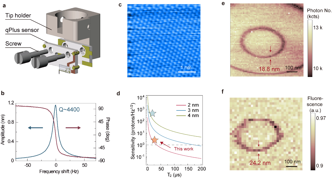
Figure 2 (a): The new-type qPlus sensor for ambient conditions. (b): Frequency sweep of the new-type qPlus sensor. (c): STM image on a HOPG surface under the ambient condition with atomic resolution. (d): The sensitivity of NV has been enhanced up to the level of a single proton by the strong local electric field of qPlus tip. (e): Scanning field-gradient imaging of magnetic field from a magnetized qPlus tip. (f): Scanning field-gradient imaging of electric field from a conductive qPlus tip.
The quality factor of the new-type qPlus sensor is up to ~4400 (Figure 2, a and b). On the one hand, this system can realize atomic resolution on HOPG’s surface (Figure 2c). On the other hand, based on the strong local electric field of the qPlus tip, this system can not only realize the charge state control of a single shallow NV with nanoscale resolution but also efficiently suppress the magnetic noise near the diamond surface, leading to the enhanced sensitivity by nearly two orders of magnitude up to the level of a single proton (Figure 2d). Furthermore, based on a single NV center, this system also demonstrates the scanning field-gradient imaging of magnetic field and electric field from the SPM tip, with a spatial resolution of ~20 nm (Figure 2, e, and f).
This new kind of scanning quantum sensing microscope has broken through the sensitivity limitations of conventional SPM in detecting weak electric and magnetic fields. It paves the way for developing the method for imaging, spectroscopic measurement, and manipulation of electric/magnetic signals with nanoscale/atomic resolution, which is promising in extensive applications in physics, chemistry, material science, and biology.
Ying Jiang and Dr. Ke Bian are the corresponding authors. Dr. Ke Bian, Dr. Wentian Zheng (Now a Smalley-Curl postdoc fellow at Rice University), and the PhD student Xiakun Chen are the co-first authors. This work was financially supported by the National Natural Science Foundation of China, the Ministry of Science and Technology, the Beijing Municipal Science & Technology Commission, the New Cornerstone Science Foundation, and the China Postdoctoral Science Foundation.
The information and links for this paper: https://doi.org/10.1063/5.0202756
Related Patents:
[1] Ying Jiang, Ke Bian, a new kind of qPlus sensor, 2020-9-4, China, ZL202021914791.6
[2] Ying Jiang, Ke Bian, Wentian Zheng, A three-dimensional stage for positioning the objective lens and its installation method, 2020-9-4, China, ZL202010922734.0
[3] Ying Jiang, Ke Bian, Wentian Zheng, An electric-controlled stage for adjusting vector magnetic field and its installation method, 2020-9-4, China, ZL202010922767.5